
IBM officially introduced the world's first sub-1 nanometer chip, specifically a 0.7 nm or 7 angstrom transistor node. By packing nearly 100 billion transistors onto a piece of silicon roughly the size of a fingernail, this milestone essentially doubles the transistor density. This could result in up to 50 percent better computing performance or a 70 percent reduction in power consumption compared to 2 nm chips.
So, how did they do it and what’s next?
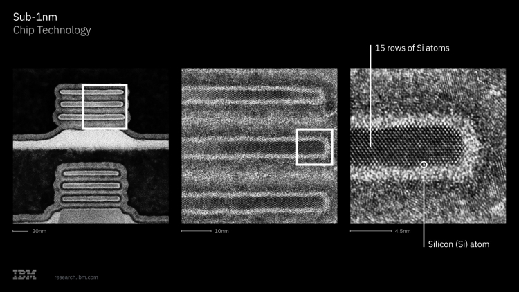
Researchers designed a unique feature called "nanostack" architecture, which represents the industry's first 3D sequential integration layout where transistors are stacked and staggered vertically. This approach does more than save physical space, it also gives engineers the freedom to combine entirely different materials across layers to optimize individual transistor performance.
Testing has already proven fruitful, showing a 40 percent scaling improvement in SRAM. After going below 1nm to 7A or angstrom, we will be left with 5A, 3A and eventually 1A. However, many expect this to go in tandem with more 3D nanostacks as well. IBM is planning a pure-play quantum foundry called Anderon with below 1nm production expected in 5 years.
For the normal electronics user it eventually means we could have devices that perform better and last longer. It might eventually trickle down to us, but we expect data centers to get them first. What do you think? Let us know your thoughts in the comments below, and stay tuned to TechNave.com for more on tech.


COMMENTS